13
LTC3445
3445fa
micro-steps. The table below shows the register settings
and corresponding slew rates.
REG1 [1:0]
SLEW RATE (mV/?/SPAN>s)
00
11.3
01
7.5
10
3.8
11
0.9
It should be noted that during DAC transistions, PGOOD
fault reporting is disabled.
LDO OPERATION
Adjustable Operation
The LTC3445 contains two 50mA LDOs with an output
voltage range of 0.6V to (V
CC2
0.3V). The output voltage
is set by the ratio of two external resistors as shown in
Figure 1. Each LDO servos the output voltage (Pin LDOx)
in order to maintain a feedback voltage (Pin LDOxFB) of
0.6V. The current in R1 and R2 is then equal to 0.6V/R2.
The regulated voltage is equal to:
V
OUT
= (0.6V/R2) " (R1+R2)
Frequency Compensation
The LT3445 is frequency compensated by an internal
dominant pole. An output capacitor of 2礔 to 10礔 is
usually large enough to provide good stability. In order to
insure stability, a feedforward capacitor may be needed
between the output pin and the feedback pin. This cancels
the pole formed by the stray capacitance in large value
feedback resistors. Also, a feedback capacitor minimizes
noise pickup and improves ripple rejection.
PowerPath OPERATION
The output of the PowerPath (V
CC
BATT) is controlled by
a combination of three inputs: main battery (V
CC1
), V
TRACK
,
and V
BACKUP
.
OPERATIO
(refer to Figure 1)
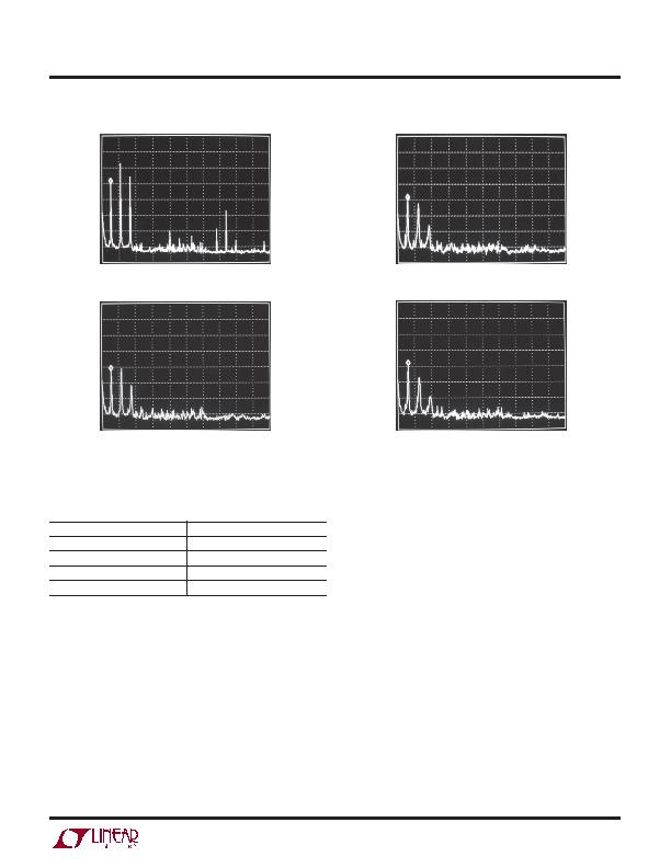
SPR = 00 (Spread Spectrum OFF)
NOISE
10dBm/DIV
SPR = 01
NOISE
10dBm/DIV
START FREQ: 100kHz, RBW: 10kHz, STOP FREQ: 30MHz
START FREQ: 100kHz, RBW: 10kHz, STOP FREQ: 30MHz
SPR = 10
NOISE
10dBm/DIV
SPR = 11
NOISE
10dBm/DIV
START FREQ: 100kHz, RBW: 10kHz, STOP FREQ: 30MHz
START FREQ: 100kHz, RBW: 10kHz, STOP FREQ: 30MHz
Figure 4. LTC3445 Output Noise Spectrum
发布紧急采购,3分钟左右您将得到回复。
相关PDF资料
LTC3446IDE#PBF
IC REG TRPL BCK/LINEAR 14-DFN
LTC3537EUD#TRPBF
IC REG DL BST/LINEAR SYNC 16-QFN
LTC3541EDD#TRPBF
IC REG DL BCK/LINEAR SYNC 10-DFN
LTC3670EDDB#TRPBF
IC REG TRPL BCK/LINEAR 12DFN
LTC3672BEDC-1#TRPBF
IC REG TRPL BCK/LINEAR 8-DFN
LTC3700EMS#TRPBF
IC REG DL BUCK/LINEAR 10MSOP
LTC4151HMS#TRPBF
IC PWR MONITOR MS 80V SD 10MSOP
LTC4210-2CS6#TRM
IC CONTROLLER HOT SWAP TSOT23-6
相关代理商/技术参数
LTC3446
制造商:LINER 制造商全称:Linear Technology 功能描述:Monolithic Buck Regulator with Dual VLDO Regulators
LTC3446EDE
制造商:LINER 制造商全称:Linear Technology 功能描述:Monolithic Buck Regulator with Dual VLDO Regulators
LTC3446EDE#PBF
功能描述:IC REG TRPL BCK/LINEAR 14-DFN RoHS:是 类别:集成电路 (IC) >> PMIC - 稳压器 - 线性 + 切换式 系列:- 标准包装:2,500 系列:- 拓扑:降压(降压)同步(3),线性(LDO)(2) 功能:任何功能 输出数:5 频率 - 开关:300kHz 电压/电流 - 输出 1:控制器 电压/电流 - 输出 2:控制器 电压/电流 - 输出 3:控制器 带 LED 驱动器:无 带监控器:无 带序列发生器:是 电源电压:5.6 V ~ 24 V 工作温度:-40°C ~ 85°C 安装类型:* 封装/外壳:* 供应商设备封装:* 包装:*
LTC3446EDE#TRPBF
功能描述:IC REG TRPL BCK/LINEAR 14-DFN RoHS:是 类别:集成电路 (IC) >> PMIC - 稳压器 - 线性 + 切换式 系列:- 标准包装:2,500 系列:- 拓扑:降压(降压)同步(3),线性(LDO)(2) 功能:任何功能 输出数:5 频率 - 开关:300kHz 电压/电流 - 输出 1:控制器 电压/电流 - 输出 2:控制器 电压/电流 - 输出 3:控制器 带 LED 驱动器:无 带监控器:无 带序列发生器:是 电源电压:5.6 V ~ 24 V 工作温度:-40°C ~ 85°C 安装类型:* 封装/外壳:* 供应商设备封装:* 包装:*
LTC3446EDE-PBF
制造商:LINER 制造商全称:Linear Technology 功能描述:Monolithic Buck Regulator with Dual VLDO Regulators
LTC3446EDE-TRPBF
制造商:LINER 制造商全称:Linear Technology 功能描述:Monolithic Buck Regulator with Dual VLDO Regulators
LTC3446IDE
制造商:LINER 制造商全称:Linear Technology 功能描述:Monolithic Buck Regulator with Dual VLDO Regulators
LTC3446IDE#PBF
功能描述:IC REG TRPL BCK/LINEAR 14-DFN RoHS:是 类别:集成电路 (IC) >> PMIC - 稳压器 - 线性 + 切换式 系列:- 标准包装:2,500 系列:- 拓扑:降压(降压)同步(3),线性(LDO)(2) 功能:任何功能 输出数:5 频率 - 开关:300kHz 电压/电流 - 输出 1:控制器 电压/电流 - 输出 2:控制器 电压/电流 - 输出 3:控制器 带 LED 驱动器:无 带监控器:无 带序列发生器:是 电源电压:5.6 V ~ 24 V 工作温度:-40°C ~ 85°C 安装类型:* 封装/外壳:* 供应商设备封装:* 包装:*
